Architecture and Features of PIC18F4550
Architecture of PIC Microcontroller (PIC18F4550)
- Complete Video Course on PIC18F4550 Microcontroller
- Introduction: Architecture and Features of PIC18F4550 Microcontroller
- 1. CPU Architecture
- 2. Memory Organization
- 3. Oscillator and Clock System
- 4. I/O Ports
- 5. Timers and Counters
- 6. Communication Interfaces
- 7. Analog Features
- 8. Capture/Compare/PWM (CCP) Modules
- 9. Special Function Registers (SFRs)
- 10. Interrupt System
- 11. Power Management Features
- 12. Development and Programming
- Applications
- Summary (Architecture of PIC Microcontroller: PIC18F4550)
- Learn More
- Complete Video Course on PIC18F4550 Microcontroller
- 💬Frequently Asked Questions (FAQ)
Would you like to join our comprehensive practical video course on the PIC18F4550 Microcontroller?
Complete Video Course on PIC18F4550 Microcontroller
Introduction: Architecture and Features of PIC18F4550 Microcontroller
Before we start programming and configuring modules, it’s essential to understand the architecture that powers the PIC18F4550 microcontroller. This microcontroller from Microchip Technology belongs to the PIC18 family and is widely used in industrial, educational, and USB-based embedded applications.
PIC18F4550 offers high performance, low power consumption, and excellent peripheral integration – making it an ideal choice for both beginners and professionals. Go through the picture, the architecture of PIC18F4550.
Architecture of PIC Microcontroller (PIC18F4550)
For a clear view, download the datasheet and see page 11: Download PIC18F4550.pdf
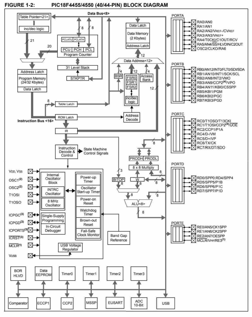
1. CPU Architecture
PIC18F4550 is based on an Enhanced Harvard Architecture, meaning:
- Separate buses for program memory and data memory
- Allows simultaneous instruction fetch and data access
- Results in faster execution and improved performance
It features a pipelined architecture, where:
- One instruction is fetched while the previous is executed
- Most instructions execute in a single clock cycle
🔹 Key CPU Specs:
- 8-bit CPU
- 16-bit instruction width
- High-speed 10 MIPS performance at 40 MHz
- 31-level deep hardware stack
2. Memory Organization
PIC18F4550 includes three main types of memory:
| Memory Type | Size | Description |
|---|---|---|
| Program Memory (Flash) | 32 KB | Stores firmware code |
| Data Memory (RAM) | 2 KB | Used for variable storage during program execution |
| EEPROM | 256 Bytes | Non-volatile storage for data retention |
All memories are separately addressed due to the Harvard design.
3. Oscillator and Clock System
Supports various clock options:
- External Crystal (up to 48 MHz with PLL)
- Internal oscillator (up to 8 MHz)
- PLL multiplier for USB applications requiring precise timing (48 MHz USB clock)
4. I/O Ports
- 5 ports (PORTA–PORTE), total 35 I/O pins
- Each pin can be configured as input or output
- Most pins are multiplexed with peripheral functions such as ADC, PWM, UART, etc.
5. Timers and Counters
Includes 4 timers:
- Timer0, Timer1, Timer2, Timer3
Each can operate in timer or counter mode and can be driven by internal or external clock sources.
6. Communication Interfaces
PIC18F4550 supports multiple communication protocols for embedded networking:
| Protocol | Description |
|---|---|
| USART (UART) | Serial communication with PCs or modules |
| SPI | High-speed synchronous serial interface |
| I²C | Multi-master, multi-slave communication |
| USB 2.0 | Full-speed (12 Mbps) interface for PC connectivity |
7. Analog Features
- 10-bit ADC with up to 13 analog channels
- Comparators for analog comparison
- Ideal for sensor interfacing and data acquisition applications
8. Capture/Compare/PWM (CCP) Modules
- Two CCP modules (CCP1 and CCP2)
- Generate PWM, measure pulse width, and compare events
9. Special Function Registers (SFRs)
Control the operation of all peripherals.
Each module (Timer, ADC, UART, etc.) has its own SFRs for configuration and control.
10. Interrupt System
- Up to 20 interrupt sources
- High and Low priority levels for efficient response handling
- Ideal for real-time embedded applications
11. Power Management Features
- Sleep mode for low power consumption
- Idle mode for partial shutdown of peripherals
- Watchdog Timer (WDT) to reset MCU in case of software fault
12. Development and Programming
PIC18F4550 supports various development environments and tools:
- MPLAB X IDE
- XC8 Compiler
- PICkit 3/4, ICD 4 for programming and debugging
Applications
- USB-based devices (keyboards, mice, data loggers)
- Sensor-based embedded systems
- Industrial automation and motor control
- Student and research projects
Summary (Architecture of PIC Microcontroller: PIC18F4550)
The PIC18F4550 microcontroller is a robust and versatile device with advanced peripherals, large memory, and high-speed architecture. Understanding its internal architecture provides a strong foundation for developing complex embedded applications efficiently.
Learn More
🎓Would you like to join our comprehensive practical video course on the PIC18F4550 Microcontroller?
➡️ Start Learning Now at “Master PIC18F4550 Programming“
Complete Video Course on PIC18F4550 Microcontroller

💬Frequently Asked Questions (FAQ)
A1. It uses an Enhanced Harvard Architecture with a pipelined instruction cycle.
A2. It has 32 KB of Flash memory for storing program code.
A3. Yes, it supports Full-Speed
A4. The microcontroller provides 35 general-purpose I/O pins.
The VUSB pin provides a regulated 3.3V output for the USB transceiver — connect a 470nF capacitor between VUSB and GNA5. It combines multiple peripherals (ADC, USB, UART, SPI, PWM) and has simple programming tools, making it perfect for hands-on embedded learning.D.


